(c) klausmobile 2000
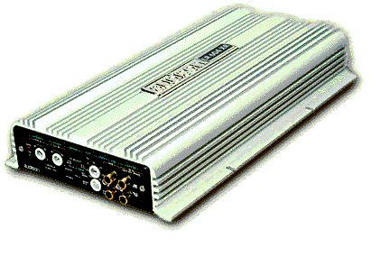
Of the few car amplifiers I tested, gutted, decyphered and fixed, this one seems to be the best in design quality. Too many car amps (although solidly built) are apparently designed by computer class students - too many traces, too many vias, absolutely wrong component placement etc. And on schematic level, their different functional parts look like a newspaper clip collection. If the amp is built on bipolar transistors, and the preamp/crossover on FETs, then they were designed by different guys, right? Not this amp. Here, a strong, experienced designer's hand is evident from schematic to parts layout, PCB routing and general assembly. Which leads to one of the lowest failure rates (don't quote me on this although it's common knowledge in repair industry) and a surprisingly good sound from a $50 per channel device. A unit worth a Web page. LR series - Audison's junior - was formally discontinued in 1999, just to be repackaged under 'Millenium' series name. Oh, and if you think Audison is another Macau or Shanghai sweatshop it's not, it's 100% Italian.
1. Layout
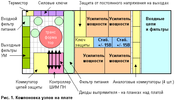
Narrow heat sink dictates board shape. Quite logically, power supply and power output are on one side, RCA inputs and XO switches on the other. Which also means that acoustic output traces run directly under DCDC transformer. Anyway, the form factor doesn't allow a third option. DCDC converter and analog parts are separated with a wall of filter caps (on internal power rails). Parts are quite densely packed; rectifier diodes are mounted on flat individual heatsinks above the PWM controller ICs (I understand the designer: there is no space left on the upper contact strip, and placing diodes on the lower one will need long, noisy and lossy power traces). This, as well as mica+grease transistor pads, will add difficulties to repair man, actually I replaced mica with long silicon strips. It is good to see all marked components coming from decent makers - Philips, SGST, Motorola, Elna (although not Cerafines - RE2, RE3 series for analog and RSG series for switcher).
2. Too many blocks...
Compared to home gear, where amps sometimes have no speaker protection, or thermal shutdown, a car amp MUST have these and other 'unnecessary' things to survive. I haven't yet seen a car amp with blown output devices, but plenty with a dead DCDC converter. They saved pennies on protection, poor bastards... This has nothing to do with LR604 - I was just curious to see what's inside.
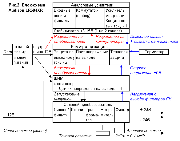
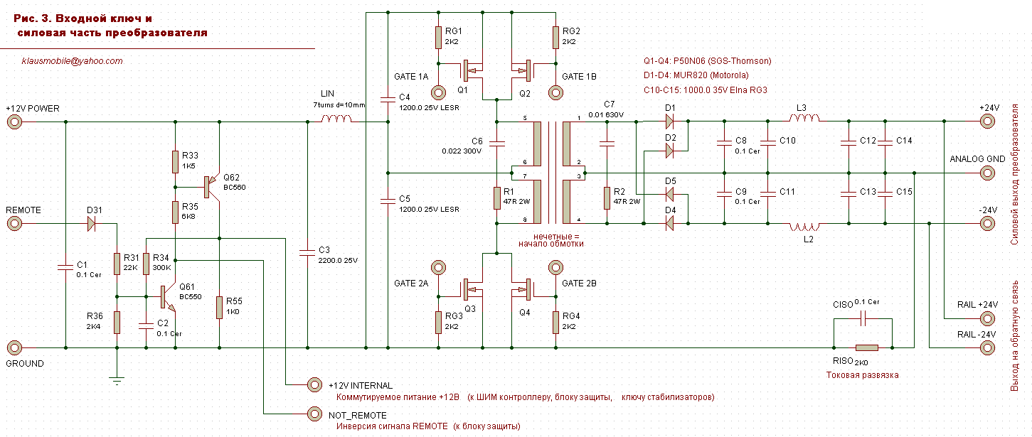
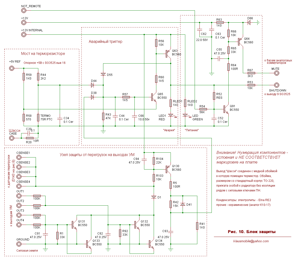
Input REMOTE line switches on a low-drop input switch, that powers a low-current internal 12V rail. This switch goes on at +8V with 1V hysteresis, powering low-power PWM controller IC pin (it has two Vdd pins, low and high current), protection switches and multiplexer, and a switch controlling regulators in the power amp section. High-current PWM controller pin (gate drivers Vdd) is powered from main +12V input via a series resistor.
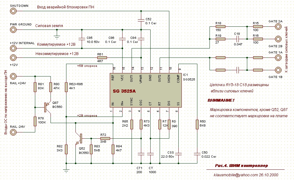
PWM controller is based on a derelict SG3525A, in voltage feedback mode. A traditional push-pull DCDC converter has three features to note. One is an RC ground current breaker, isolating power ground from analog ground, this is not uncommon. Another is a smart heat-sensitive duty cycle limiter. And a third is an oddest gate drive network (see below).
Protection is built along three lines: (a) Overheat shutdown (b) Instant output current in each channel (c) DC at amplifier outputs. Protection output has two alert modes: (a) Shutdown - highest all-out priority, kills DCDC power (b) Output Disable - disconnects analog switches, keeping DCDC unit running.
The only ICs are: PWM controller and opamps in the crossovers section. All protection circuitry is discrete, actually taking less space than alternative designs on LM339 and CMOS logic. Despite component density, PCB traces are quite thick, with decent spaces, and a surprisingly low via count (compared to PPI, Soundstream, MTX et al).
3. Power Supply
... Schematic 1. Input switch and Power DCDC Inverter
... Schematic 2. PWM Controller
The designer seems to love the discrete, low drop npn-pnp switch circuit. There are four such switches in LR604, one is the input power switch.
The odd transistor in PWM controller's error amp input (Q52) puzzled me, and my explanation is: As temperature inside the cabinet rises, Q52's threshold B-E voltage falls, and maximum PWM duty cycle decreases. Another safety feature.
Voltage feedback network has quite high resistance, and it's current doesn't affect ground breaker performance. It might look asymmetrical but it's not, both rails have equal effect on error amp. Note the abundance of ceramic caps around all DC lines.
Normally a designer wants as much current as possible in the gate drive line; some driver ICs pump out 12A through a Dip8 package. But here, there's an added resistance - min. 87 max.200 Ohm to each gate. Why? Ask the Italians.
Transformer core has very thin crossection, so it can accomodate beefy litz windings (each strand has seven, I believe, 0.8mm copper wires). 12V filter caps are placed as in the text book, immediately between FET's source and the transformer center tap, keeping current path as short as possible (I'd say, 4-6 centimeters of copper traces plus FET pins plus primary windings). These caps are low-ESR Elna RSG series (105C, Longlife). Input choke is wired with a single 2.2mm copper wire on an upright ferrite rod. Copiuous solder blobs on the PCB power traces decrease resistive losses.
Secondary is a plain center-tap bridge rectifier. No snubbers across diodes, but one snubber across secondary outputs and one across primary. Rectifier pumps directly into an Elna electrolytic, then through chokes into another cap bank.
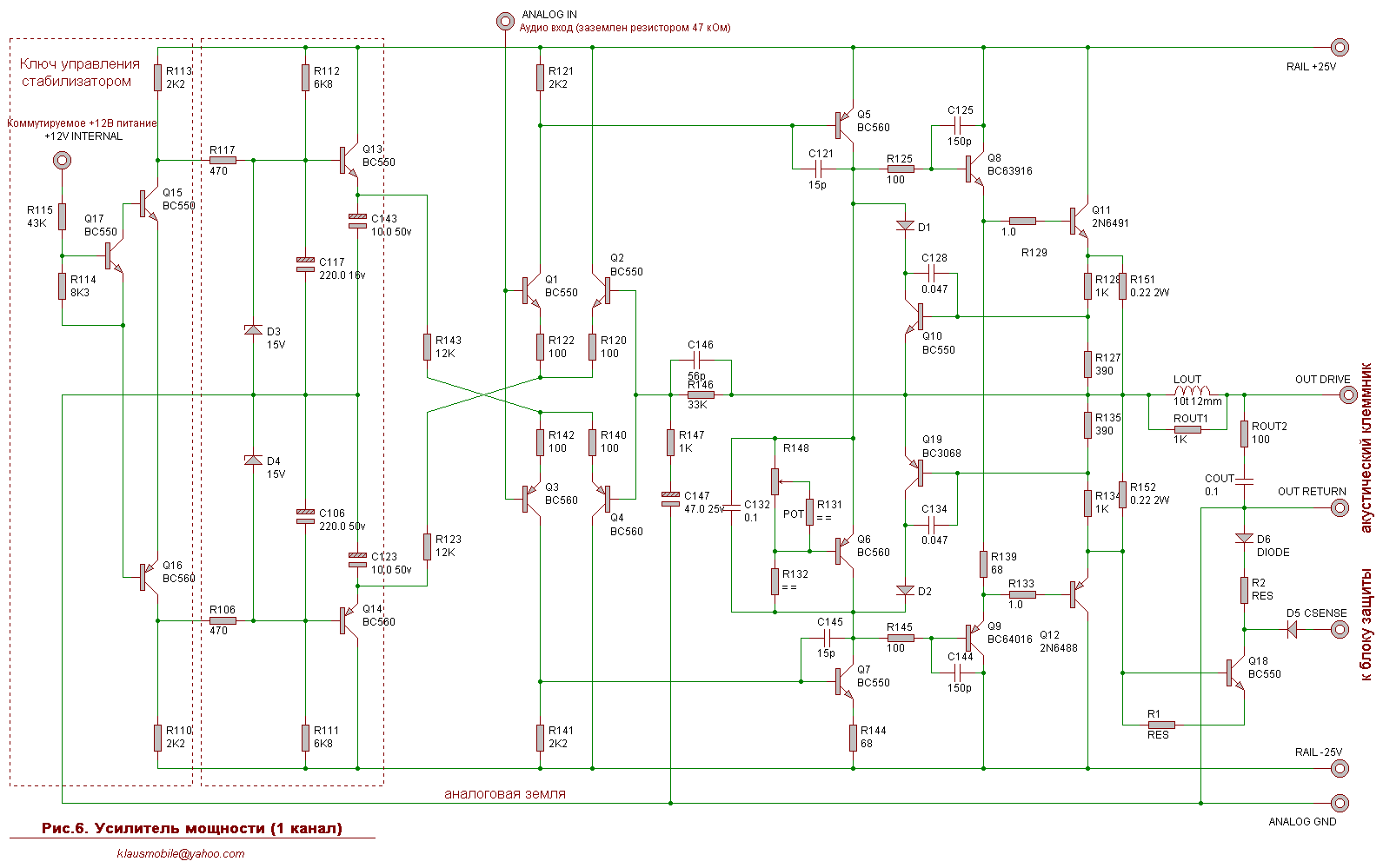
4. Power Amps
... Schematic 3: Power amp, including regulators and switches
This, I believe, is the circuit employed by 75% of car amps, but then why do they sound different ? :)). One TO220 transistor per channel per leg means that the rated 2*180W RMS into 4 Ohm bridged numbers are ... well... too optimistic. It shouldn't run such loads even on transients. Output is biased at 20 mA.
Each power amp takes 6 cm of heat sink's contact strip. Bias transistor and pre-output transistors (TO-92 cases) are also clamped to the heatsink with a special wave-shaped clip, so that three devices take as much space as one TO220 device.
Note that all four output channels are services by one regulator control switch and two regulator sets.
5. Protection circuits
Protection circuit is distributed all over the board - current sensors are placed by the power amps, two DC sensors - separately in the analog part of the board, protection triggers - close to the PWM controller. 4 current and 2 DC sense lines are joined in open-collector AND logic; low state in each line opens Q93 (normally closed) and, thru a Q65-Q63 switch, sends high Shutdown signal to PWM controller. Trigger latches up in Shutdown mode unless REMOTE signal is switched on and off again. Note the smart timing filters in Q65 base chain.
Shutdown also controls Q91-Q64 switch that turns muting circuits to open (high level) and close (low level). R65-C55-R64-D66 enable delayed turn-on and quick turn-off in normal operation.
6. Credits
Thanks to and for review and corrections. Thanks to Wiha, Hakko and Fluke for excellent work tools.
And thanks to . This a rare example of a mass product where individual signature of a competent designer is evident in every small fragment. Yes they had to cut costs and corners and still it's a very reliable, and good sounding, component. Just don't expect a 4*40 wpc amp to drive your 2 Ohm subwoofer, it's made for more delicate jobs.
Index in Russian - Index in English - Mail